

Focusing nanoplasmonics
Plasmon nanolasers and Plasmon optical tweezers
Angela S. Camacho
Physics Departament, Universidad de los Andes, Bogotá Colombia
E-mail: acamacho@uniandes.edu.co
Nanoplasmonics is a fundamental tool of nanotechnology. The use of electrons instead of light brought an enormous step in this direction and therefore the interest in studying and controlling electrons in very small particles: nanoparticles, specially metallic ones, where a dramatic increase of the near field has been observed. This effect is explained as an interaction between the electronic collective excitaction in the particle (plasmon) and light, which can avoid the diffration limit prohibition and allows to see and study extraordinary small objects in spite of the diffraction limit. Two interesting applications are presented related with the nanoplasmons such as laser effect due to the high near electric fields that implies great amplification properties and on the other side their ability to create nanocavities, where the tiny forces present in the nanosystems are able to manipulate very small objects like molecules and cells.
The main idea of radiation nanofocusing was first proposed in 1997 [1], but only after a decade it was posible to demonstrate this fascinating phenomenon. This can be understood if considering that it was necessary to develope fabrication of metal nanostructures and their optical characterization at the nanoscale. Since the diffraction limit of light restricts the minimum focal spot size achievable using a dielectric lens to greater than half the wavelength in the medium, the minimum focal spot size for a nanofocusing structure can be as small as a few nanometres, being limited mainly by the atomic structure of matter. This makes nanofocusing an essential link between diffraction-limited optics and nanoscale structures or even individual molecules. In addition, it was also necessary to realize efficient coupling of radiation into suitable plasmon modes.
The very beginning of nanotechnology dates back to 1959 when Richard Feynman introducing his lecture at Caltech said: “There is plenty of room at the bottom!”. It was actually the beginning of the history of what is now known as nanoscience. AT THE BOTTOM means a world billion times smaller than our basic unit of measurement: the meter. This opens the door to the nanoworld of amazing natural phenomena that occur only in this size range. The sizes at the bottom mean much place (plenty of room). These are systems consisting of hundreds to thousands of atoms that certainly can be seen with our own eyes. That seems like science fiction! It is the twenty-first century science. The world micro, a million times smaller than a meter, was already dominated by using and controlling the electrons in microstructures. This was the miracle of the second half of the twentieth century, the miracle that reached to share Feynman, though his vision allowed him to think about how to shrink even one thousand times more the size of the structures, the nanoscale is what he called AT THE BOTTOM!!
Feynman´s proposal in his famous 1959 seminar was to write the Encyclopedia Britannica on the head of a pin, what challenged the audience to imagine if that were possible and how to achieve it. How many times should the size of the letters decrease? The answer is 25000 times and then how to read them. Is that physically possible? May be illuminating with light. But the diffraction limit of light can only resolve objects sized approximately equal to half of the wavelength of light used and the human eye can only resolve down to 20 microns.

Figure 1. Richard Feynman, Waltham 1984. CC BY-SA 3.0 Copyright Tamiko Thiel 1984.
Another way to solve the problem is using electrons instead of light because they can achieve gains of 10 million times in an electron microscope [2] while the usual optical microscope increases the order of a thousand times. On the other hand, understanding and controlling electrons have enabled a breakthrough in science and technology. When a piece of matter is divided more and more, it can reach the nanometer scale and its physical properties change because its ratio area to volume increases as it becomes smaller and smaller and then the surface electrons are becoming responsible for the interactions. When electrons are confined to a nanometric volume their energies become quantized (discrete) like in natural atoms. The question is, the electrons behave in these artificial atoms in the same way as in natural atoms?
Plasmons
Light falling on a nanoparticle can be absorbed and the inner electrons make transitions to higher energy states in the same way as they do inside the atoms. Moreover, if the particle is metallic all valence electrons simultaneously interact with the light and these behave like a single particle which is known as a plasmon.
A plasmon is created when light hits the surface of the conductor under certain specific conditions. A plasmon in a wave of the electronic fluid into a piece of metal such as the waves on the water surface of a pond are collective modes of the water molecules in the liquid. Plasmonics is the study of the interaction of light with the free electrons of the metal. When did plasmonics start and has modern plasmonics has been developed? The most important contributions of what is called plasmonics come from long ago. It’s been more than a century since Gustav Mie in 1908 was first interested in the subject [3]. The interest was sparked again just over two decades ago but this time at the nanoscale, in the nineties there were new instruments such as the scanning optical near-field microscopy which is based on the property with surface plasmons to create electric fields very strong near the surface of the metal and techniques as resolved spectroscopy femto-seconds which allowed to control nano-sized structures, and even individual nanoparticles [4]. Almost everything about photonics can be considered in terms of plasmonics and their potential applications are everywhere.

Figure 2. Gustav Mie (1869-1957) Lic: CC-BSA-2.5,2.0,1.0
All luminous object shows besides the far field emitting and usually observed, the near field surrounding it as a very thin layer of skin and is much greater than the incident field [5]. When a metal or the tip of a glass probe is inserted the object with a higher resolution than with a conventional microscope can be observed. The optical information is obtained from the intensity of scattered light. This field scanning microscopy has opened new areas of research: Surface Enhancement Raman Spectroscopy (SERS), Plasmonics and optical antennas. As for the high spatial location, no other systems with the same qualities in this range are known. The features that allow to change the properties of emission and excitation open a long way before exploring their potential. Small volumetric modes and high spontaneous emission when the atoms are in a resonant cavity are great reasons to use plasmons.

Figure 3. Metal nanoparticles support surface plasmons: oscillations of the free electrons at the nanoparticle surface.
Mechanisms of interactions
Two mechanisms dominate the interaction of a metallic nanoparticle with light: first, the rapid response of the conduction electrons moving almost freely in the material when they experience an external electromagnetic excitation and second the contribution of internal transitions between discrete energy levels to the optical response of the material, which is getting more important as the nanoparticles sizes decrease. On the other side, plasmonic colors depend on the size and shape of the nanoparticles. A huge enhancement of the near field known as SERS has been reported for the first time in 1978 [6] and sparked great excitement as plasmon was attributed to the combined substrate with chemical effects. In 1997 detection of a single natural molecule was reported [7]. The possibility of obtaining chemical signals from single molecules is used for the study of biochemical pathways and dynamics still supramolecular chemistry within living cells. In spite of the dramatic increase of the near field for several orders of magnitude in arrays of nanoparticles [8], there have been only few experiments examining this field effect on the nanoparticle size and the distance between them (interdistance).

Figure 4. Surface plasmon polaritons are electromagnetic waves (metal-dielectric interface) and charge motion in the metal.
In a more recent very interesting experiment [9], in which no light is used but instead a beam of electrons is sent to measure its energy loss when these electrons interact with the nanoparticles at different sites inside and outside. The plasmon resonances were clearly observed, in the center, on the surface and at a half radius distance in very small nanoparticles. The resonances at the surface are the optical response of localized surface plasmons that are the source of the extraordinary increase in the near field and are involved in interactions with the environment and with other neighboring nanoparticles. However, the number of electrons involved in these excitations decreases as the nanoparticle size decreases and approaches the atomic scale.
Nanofocussing
An important characteristic of a nanofocusing structure is its ability to achieve strong spatial surface plasmon localization and large local field enhancement near the tip. It is thus, important to optimize their structures so as to maximize the localization and enhancement of the local field. There are several levels of such optimization. First, the atomic structure and spatial dispersion (nonlocal response) of the material impose fundamental physical limits on the maximum achievable localization and field enhancement at the tip. Material properties limit the minimum practically attainable tip radius. This also limits the localization of the surface plasmon field near the structural tip to a spatial region of about a few nanometres [10].
One way to achieve nanofocusing is to design nanocavities, where both localization and field enhancement are optimized. In a very nice experiment, that combine, these two conditions, two atomic force microscopes (AFM), whose tips are gold-nanoparticle, are oriented tip-to-tip. The tip apices define a nanocavity supporting plasmonic resonances that have been created via strong coupling between localized plasmons on each tip. This dual AFM tip configuration provides direct electrical connection to the tips, enabling simultaneous optical and electrical measurements. The tips are in free space. This arrangement provides spectroscopic characterization of the tip–tip plasmonic nanocavity throughout the subnanometre regime. The inter-tip separation is initially set to 50 nm and then reduced while recording field scattering spectra and direct currents simultaneously [11].
When two metallic nanoparticles are too close, their surface plasmons get coupled and can appear new entities called plasmon molecules, because they show bonding and antibonding states characteristic of natural molecules. These plasmonic states allow a tunneling effect coupling characteristic which means that the plasmons set a kind of bridge between the two particles. Interesting is that this typical behavior is easily described within a simple model of an electron confined in a sub-nanometric sphere. Jan Mertens et al. [12] used a gold nanoparticle of 80 nm on a graphene sheet to observe the two plasmonic modes, the minimum possible distance between the particle and its image. Indeed, they detected two lowest energy plasmon modes, which disappear when more than one sheet are placed. The use of graphene as a gate to tune the plasmonic coupling to fix the precise separation of plasmonic nanostructures allows: a) control the buildup of localized intense optical field, b) tune the resonance energies and c) allow the identification of molecules captured within such spaces, to femtomolar levels. Structural tapering is an essential characteristic of nanofocusing structures and ensures gradual concentration of the surface plasmon energy into a nanoscale region.
Plasmon Laser
When the laser was developed in the 50’s it was branded as a solution looking for a problem. Today it is recognized as one of the most important inventions of the twentieth century that, in just a few decades of technology, has progressed from Ruby lasers of centimeter length to mass production of semiconductor lasers and recently has become a dump attention towards development of lasers with nanoscale dimensions. The last 10 years have provided a number nanolasers of both fundamental and applied innovations. However, an essential ingredient in the technology that has been missing is the ability to emit unidirectional beam. Teri Odom and his colleagues at Northwestern University showed that a network of plasmons in plasmonic nanocavities arrangements can be used to create these light beams [13].
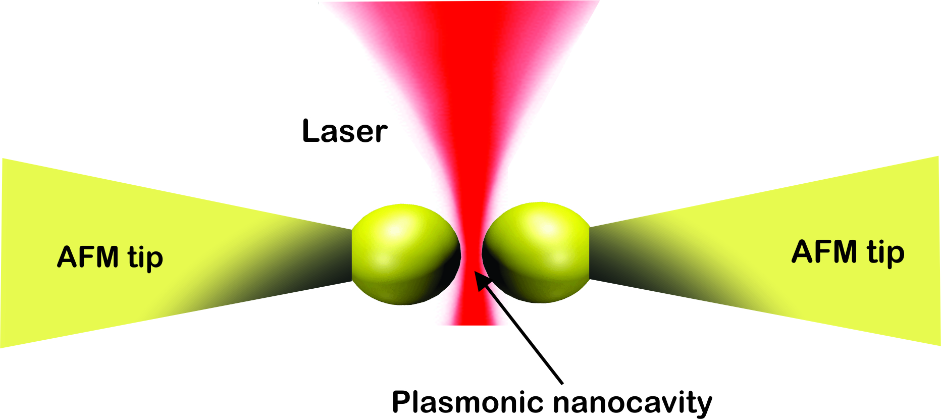
Figure 5. Plasmonic nanocavity. Two tip apices define a nanocavity supporting plasmonic resonances that have been created via strong coupling between localized plasmons on each tip. Image adapted from [11].
Lasers are based on two principles: 1) A photon traveling through a laser medium generates a second photon by stimulating radiative decay of an emitter. Repeating this process results in stimulated emission optical amplification and eventually the laser action. 2) These photon multiplication events are entirely consistent, that is, all the emitted photons have the same frequency, direction and phase as the first photon. However, if the light can propagate in any direction in the gain medium, it could go out in any direction. To avoid this problem, most centimeters lasers use an active medium between two reflective mirrors such that only electromagnetic waves having a specific direction and phase selected to be facing out when a certain intensity is achieved. The development of photonic crystals, which means periodic optical nanostructures, has given rise to laser action at small scales. The small group velocity that characterizes these modes allows control of the direction and the polarization of the laser over a large area, which is a basic characteristic of these lasers emitting from the surface of a photonic crystal.

Fiugure 6. Lattice surface plasmons enable unidirectional emission of coherent light. Image adapted from [14].
More recently, nanoplasmonics has offered the ability to access even more small systems due to the fact that surface plasmons are not subject to the diffraction limit. Large local fields associated with surface plasmons give rise to significant growth of light-matter interaction strength, which in turn dramatically stimulates the optical amplification given by the gain medium positioned in the vicinity of plasmonic field interaction. This allows to completely compensate the intrinsic loss of metallic materials at optical frequencies and eventually induce a self-sustained oscillation in the laser system. A problem that arises in the plasmonic case is the great difference between the long-wave vector of the electromagnetic radiation and surface plasmons, which means that when light is generated, it leaves scattered in all directions. Odon and his colleagues have solved this problem using photonic and plasmonic crystals. They designed 2D periodic arrays of nanoparticles of gold and silver on a glass substrate and then immersed in a polymeric medium, which is optically pumped with infrared light. The electromagnetic coupling of many localized plasmons leads to coherent modes of the lattice of nanoparticles, which in contrast to the typical modes of a photonic crystal, feature subwavelength lateral confinement structure and therefore they do not need any additional wave guide. These photonic modes show the group velocity well into the regime of sub-wavelength, allowing directional lasing emission over large areas. In simple terms, these extended modes capture all lasing light at the nanoscale produced by each nanoparticle and issued for a distributed feedback mechanism to the outside world as a directional beam. The approach developed by Odom and colleagues also has the potential for further exploitation [14].
Plasmon optical tweezers
The most developed way to manipulate and move individual functionalized biomolecules is based on the use of an instrument called “optical tweezers” (or “optical trap”), tuned in 1970 [15] and observed in 1986 {16] by A. Ashkin et.al. Conventional optical tweezers, formed in the diffraction-limited focus of a laser beam, have become a powerful and flexible tool for manipulating micron-sized objects. Extending optical trapping to nanoscale opens new prospects in many fields of science, because nano-optical tweezers allow the ultra-precise positioning of individual nano-objects. The ability of the metallic nanostructures to control light in the subwavelength scale can be exploited to design such nano-optical traps.
Optical tweezers involve the use of a highly focused laser beam to trap and move dielectric particles without “touching” physically (as the transport beam Star Trek). The laser beam is focused by sending it through a microscope objetive. The narrowest point of the focused beam, called the beam waist, contains a very strong electric field gradient (gradient force). It turns out that dielectric particles are attracted along the gradient to the region of strongest electric field, which is the center of the beam. However, the laser light also tends to apply a force on particles in the beam along the direction of beam propagation (scattering force). Capture nano-sized objects involve the ability of controlling the interplay between these two forces and allows measuring forces as small as femtonewton, one billion times smaller than that we experience in our daily lives.
Reducing the size of objects causes two effects: 1) the magnitude of the restoring force decreases following a law of R3, which means a very weak trapping. 2) damping decreases because the viscosity is reduced. At a given temperature an increasing delocalization allows the specimen to escape from the trap. To prevent leakage, one can either increase the trapping by focusing the laser or increasing the laser intensity which means increasing the depth of the potential well, which should be at least of the order of 10 kT.
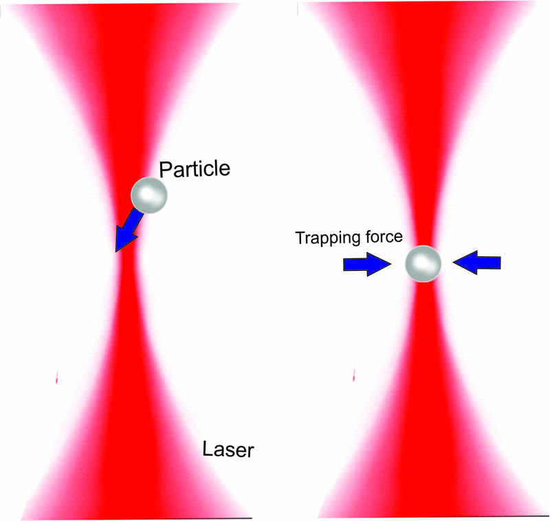
Figure 7. Optical tweezers involve the use of a highly focused laser beam to trap and move dielectric particles.
Although the diffraction limit of light prevents light from spreading beyond a fraction of the wavelength, advances in nano-optics provide alternative techniques. Evanescent fields instead of propagating fields can be concentrated below the diffraction limit. To exploit the sub-wavelength light concentration at the extremity of a sharp metallic tip to create a nano-optical trap able to immobilize dielectric objects as small as a few tens of nanometres, was proposed by Novotny [17] and Martin [18] in 1997. Plasmonic structures can be designed to couple efficiently to the light propagating and concentrating in highly localized regions of intense optical fields known as hot spots. In this way, plasmonics opens new opportunities for optical trapping.
In plasmon tweezers, a small bead becomes trapped where the field intensity is high, trapping times are several hours and the intensity of the laser can be two orders of magnitude smaller than that required to trap a bead of the same size with a conventional optical tweezers. To demonstrate that the trapping is due to plasmon polarization we can alternate two types of light polarization one that couples to plasmons and the other does not in such a way that how the bead is released can be seen. This method can be extended to catch many beads because the nanoparticles are much smaller than the spot. Conventional optical tweezers were used for particle diameters where the scattering forces are smaller than gradient forces, but particles of sub-nanometer size experiment higher gradients forces and therefore conventional optical trapping usually push mesoscopic metallic particles and Mie particles size above 1 nm away from the spot of light because scattering forces are stronger. Although several special optical tweezers are based on the strength of scattering to confine Mie particles in a potential ring, in practice, such techniques have problems with accuracy, the adjustment of the laser beams and thin regions of entrapment.
Then a universal method to trap different sized particles has not yet been found. Recently, plasmonic tweezers based on surface plasmons excited on metal nanoestrucuras have shown an increased attractive force for both dielectrics to metals offering a way to catch and manipulate metal particles.
The plasmonic tweezers, based on the highly focused field on a sheet metal excited by radially polarized light, is also called virtual plasmonic probe. So it is possible to catch both mesoscopic as Mie particles. Experiments have chosen particles in the range of 0.5 to 2.2 mm, which require large force gradients to achieve balance. It has been found as a result of numerical analysis that the total force in optical tweezers is composed of the gradient force, weak attractive forces and a repulsive strong scattering force, which has been confirmed experimentally. For plasmonic tweezers it is found that the gradient forces are stronger and dominate the repulsive force that opposes, but the gradient force is assisted by the weak scattering force acting in the same direction. The dominant gradient force originates from the near-field coupling between the surface plasmon enhanced, while the strength of scattering is due to the thrust exerted by the focused plasmon propagation. Plasmonics tweezer is capable of trapping Rayleigh particles and also particles greater than 500 nm and up to micrometers.
We have seen that hot spots or highly localized regions of intense optical fields obtained in properly designed metallic nanostructures based on surface plasmons open new opportunities for optical trapping providing nanoscale confinement and localization and therefore have applications in waveguides, coupling of transmitters and generally active functionality at nanoscale.
From a fundamental point of view, it is possible to imagine ways in which these systems could be used, for example, to generate light and matter states entangled for quantum information applications.
From a more applied perspective, the work could lead to the development of novel devices taking advantage of the strong confinement of the electric field of the surface plasmons, such as detection devices Raman or fluorescence and scalable all-optical switches operating at ultra low power levels. However, several obstacles must be overcome first. One of the most critical is the development of efficient electrically pumped laser plasmons. This certainly requires a series of innovative conceptual advances, but considering how quickly lasing technology has already been developed, perhaps be achieved soon.
References
[1] Nerkararyan, K. V. Superfocusing of a surface polariton in a wedge-like
structure. Phys. Lett. A 237, 103–105 (1997).
[2] McMullan, D. Scanning electron microscopy, Scanning 17, 175–185 (1995).
[3] Meier, S.A. Plasmonics: Fundamentals and applications, Springer (2007).
[4] Stockman, M. Nanoplasmonics: The physics behind the applications, Physics Today, February ( 2011).
[5] Inouye, Y. and Kawata, S. Near field Scanning Optical Microscope with a metallic Probe Tip, Optics Letters 19, 159 (1994).
[6] Eagen, C.F. and Weber, W.H. Phys. Rev. B 19, 5068 (1979 ).
[7] Kneipp, K., Wang, Y., Kneipp, H., Perelman, L T., Izkan, I., Dasari, R. and Feld, M.S. Single molecule detection using surface-enhanced Raman scattering (SERS) Phys. Rev.Lett. 78 1667–70 (1997).
[8] Arias, J.C and Camacho, A. Surface plasmon resonances of a few particle linear arrays, Journal of Electromagnetic Analysis and Applications 3, 458 (2011).
[9] Scholl, J., Koh, A. L. and Dionne, J.Quantum plasmon resonances of individual metallic nanoparticles, Nature 483, 421 (2012).
[10] Esteban, R., Borisov, A., Nordlander, P., Aizpurua, J. Bringing qunatum and classical plasmonic with a quantum corrected model, Nature Com. 3, 825 (2012) and Gramotnev D. and Bozhevolnyi, S. Nanofocusing of electromagnetic radiation, Nature Photonics 8, 13 (2013)
[11] Savage, K., Hawkeye, M., Esteban, R., Borisov, A., Aizpurua, J. and Baumberg, J. Nature 491, 574 (2012).
[12] Mertens, J. et. al. Controlling Subnanometer Gaps in Plasmonic Dimers Using Graphene, Nano Letters 13, 5033 (2013).
[13] Zhou, W. et al., Lasing action in strongly coupled plasmonic nanocavity arrays, Nature Nanotech. 8, 506 (2013).
[14] Bravo-Abadand, J. and García-Vidal, F. A sense of direction: Lattice surface plasmon enable large area unidireccional emisión of coherente light generated at deep subwavelength scales, Nature Nanotech. 8, 429 (2013).
[15] A. Ashkin, Acceleration and Trapping of Particles by Radiation Pressure, Phys. Rev. Lett. 24, 156 ( 1970)
[16] Ashkin, A., Dziedzic, J. M., Bjorkholm, J. E. and Steven, Ch. Observation of a single-beam gradient force optical trap for dielectric particles, Optics Letters 11, 288 (1986).
[17] Novotny, L., Bian, R. X. & Xie, X. S. Theory of nanometric optical tweezers. Phys. Rev. Lett. 79, 645 (1997).
[18] Martin, O. J. F. & Girard, C. Controlling and tuning strong optical field gradients at a local probe microscope tip apex. Appl. Phys. Lett. 70, 705 (1997).
You may also like

Quantum Dots
The past few decades have witnessed an almost exponential growth in the application of nanomaterials
read more
Aplications in photonics
Photonics, as a science, has been developing new knowledge and technology
read more
How to obtain fuel from water..
Nanotechnology as a tool to create materials that convert light into chemical energy
read more6 responses to “Focusing nanoplasmonics”
Leave a Reply
Vol 5 No 1

EVENTS


Publication


ELISCH

Nanoscale Science and Technology Center
Sponsorship
The printed publication of this magazine is financed by the Carl ZEISS Group and mnTECHNOLOGIES
you are in point of fact a good webmaster. The web site loading speed is amazing. It kind of feels that you are doing any distinctive trick. In addition, The contents are masterpiece. you have done a fantastic job on this topic!
Very efficiently written story. It will be useful to anyone who employess it, including me. Keep up the good work – for sure i will check out more posts.
adidas goodyear [url=http://www.roxshop.se/dnd.php?sv=id-1627]adidas goodyear[/url]
Hello. fantastic job. I did not imagine this. This is a remarkable story. Thanks!
christian louboutin outlet opiniones [url=http://etic-cameroun.org/amerou.php?es=christian-louboutin-outlet-opiniones]christian louboutin outlet opiniones[/url]
Hello, just wanted to tell you, I liked this post. It was helpful. Keep on posting!
I see interesting articles here. Your website can go viral easily,
you need some initial traffic only. How to get it?
Search for: ricusso’s methods massive traffic
NHKマイルC 2010 予想、オッズ、厳選買い目は?今年の狙うべきポイントを限定公開!
replica tag heuer mens watch sale [url=http://www.watchheuer.ru/fake-tag-heuer-aquaracer-grande-date-mens-watch-waf1011ft8010-p-265.html]replica tag heuer mens watch sale[/url]