

Novel Optical Design of Field Emission SEMs
To cite this article use: Boese, M., Lennz, S., Han, L., Dietl, Ch., Meyer, S., Drexler, V., Gamm, B. Novel Optical Design of Field Emission SEMs. J. Nano Sc. Tech, 4(2016)59-65
Innovations in Gemini Column, Detection Technology and Variable Pressure Technology
Markus Boese
Sabine Lenz
Luyang Han
Christian Dietl
Stefan Meyer
Volker Drexler
Björn Gamm
Carl Zeiss Microscopy GmbH
Field emission scanning electron microscopy is standard technology for high resolution imaging and different contrasting methods aiming for a comprehensive characterization of specimens. A wide range of applications is covered by classical FE-SEM technology, includ ing imaging surface sensitive and non-conductive samples without pre-treatment. The novel optical design of the Gemini column now delivers high contrast images at low voltage combined with excellent signal detection efficiency and signal-to-noise. Furthermore, an innovated concept for imaging at higher pressure ranges allows fast acquisition of crisp images in variable pressure mode with all the Inlens detectors known from high vacuum mode.
Overview of Gemini electron optics
In 1993 [1] the DSM 982, the first field emission SEM with Gemini technology, was launched. 3 – 4 nm at 1 kV. This was a benchmark for low voltage SEM
(LVSEM) and expanded the field of FE-SEM applications into low landing energies. Its major advantages are: reduced sample damage, increased SE yield and higher surface sensitivity for higher resolution thanks to smaller interaction volumes and a small beam. The Gemini optical concept incorporates the Gemini objective lens and the beam booster.
The Gemini lens is a compound magnetic-electrostatic objective lens (Fig. 1). With this type of lens, the chromatic and spherical imaging aberrations (Cc and Cs) decrease significantly with decreasing beam energy [2].
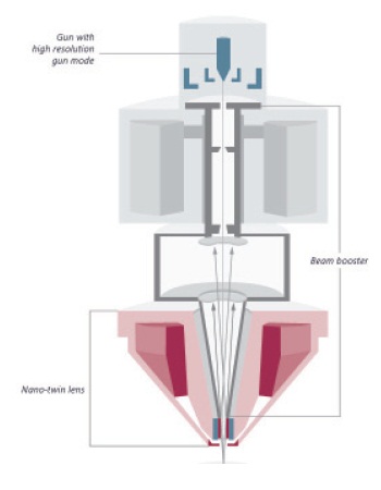
Figure 1. Schematic cross-section of Gemini optical column with new high resolution gun mode, beam booster, Inlens detectors, novel lens design (compound lens consis-ting of magnetic and electrostatic lens).
The novel optical design of the Gemini column mainly lies in innovations in gun mode and lens design.
By further optimizing geometry and electrostatic, as well as magnetic field distributions, the Gemini objective lens has been optimized even further. It now provides 1.2 nm at 500 V. In addition, no usability issues, such as additional fields at the sample, need to be taken into account, as they would occur with sample biasing.
A special gun mode was developed to The resolution was reduced chromatic aberration is further minimized to allow even smaller probe sizes and keep resolution sufficient even at voltages lower than 1 kV.
The electron optical performance is maximized while field influences at the sample are reduced to a minimum.
The novel Gemini objective lens delivers excellent imaging conditions even on challenging samples such as magnetic materials. As before, the Gemini beam booster technology (Fig. 1) guarantees small probe sizes and high signal-to-noise ratios down to ultra-low accelerating voltages.
System sensitivity to external stray fields is minimized by keeping the beam at high voltage throughout the column until its final deceleration.
Gemini technology enables high resolution at low voltage
High resolution at low voltage is needed to avoid beam damage and to balance the SE yield and beam current for charge neutrality. With the two following application examples (Fig. 2a, b), we were able to easily achieve excellent imaging conditions in charging samples like Al2O3 or in beam sensitive and charging materials like FeO(OH). In the Al2O3 sample surface, steps of one to several mono-layers can be imaged. Goethite (FeO(OH)) has nanometer sized gaps, originating from water molecules leaving the crystal during the dehydration process.

Figure 2. a) Nanometer spaced FeO(OH) crystals at imaged at 1 kV. Sample: courtesy of L. Maniguet, INP Grenoble, FR. b) Surface of a Al2O3 sphere. c) Etched silicon nano-structures imaged at 50 V beam voltage- without sample biasing. Sample: courtesy of A. Charai, Aix Marseille University, France. d) Mesoporous Silica imaged at 500 V.
Detection technology – detectors for high resolution, sensitivity and efficiency
The Gemini detection concept assures efficient signal detection by detecting secondary (SE) and backscattered (BSE) electrons in parallel. The Inlens detectors are arranged on the optical axis which reduces the need for realignment and thus minimizes time to image. The optimization of high resolution properties and detection efficiency provide high quality SEM images. The Gemini objective lens with a novel design optimizes in-lens SE detection as it not only acts as an imaging lens, but also enhances detection for secondary and backscattered electrons emitted by the sample: the electron trajectories for the detection path are further improved by
the novel design of the objective lens. Here, the in-lens SE signal is up to 20 times higher compared to classic SEM designs. This enables imaging at very low voltages and usage of fast scan speeds for high speed sample investigation.
The great flexibility of usage of different voltages is shown in Fig. 2c, d. Voltages of 500 V, or even 50 V, can be used to acquire images with a good signal -to-noise ratio. In zeolite channels can be imaged clearly down to sizes of only several nanometers (Fig. 2d). Here the combination of high resolution with good detection efficiency –both at low voltage– is essential and can be achieved without biasing the sample holder.
Moreover, the energy filtering properties of the Gemini lens are also valuable for imaging doping profiles of semicon- ductor structures with enhanced voltage contrast. It was demonstrated [3] that for the Gemini lens, this contrast can be optimized with specific high tensions and working distances by selecting only certain SE take off angles and energies.
Detection Technology – Inlens EsB detector for energy filtering and detection of low voltage BSE
A second detector on the optical axis in the column is the Inlens EsB (energy selective backscatter) detector with an energy filtering grid that enables a separation of SE and BSE. Energy filtering can be used to enhance material contrast for low loss BSE due to spectral differences [4]. This new trend in SEM of looking into spectroscopic information of the detected electrons is gaining momentum. Nagoshy et al. [5] have recently described a method using the combination of the energy filtered grid bias and the pixel-by-pixel image subtraction, thus providing the band-pass energy filtered images and extracting the material and topographic information of the specimen.
The EsB detector is an efficient BSE detector, which can be used even at low voltages. Thanks to the smaller interaction volume at low primary energies, nanostructures especially can be imaged at high resolution without being blurred by additional matrix signal. At beam voltages of 1.5 kV or lower the excellent sensitivity and resolution of the Inlens EsB de- tector can be demonstrated. Silver nano particles embedded in the Zeolite just underneath the surface are clearly visible.
Detection Technology – STEM and BSE
In addition to the in-lens detectors, improved semiconductor detectors are available for BSE and STEM (scanning transmission electron microscopy) imaging. Both are available as semiconductor, multi-segment detectors. The common feature of those retractable detectors is: angular sensitivity at fairly low voltages combined with excellent signal-to- noise ratios. The segments can be read out individually, in multiple combinations and up to four signals in parallel.
For STEM this enables the most commonly used brightfield (BF), Oriented darkfield (ODF) and High angular annular darkfield (HAADF) modes. For the BSE detector the standard modes are compositional or topographical imaging with the back scattered electrons.
The Bariumhexaferrites are magnetic nanoparticles with multiferroic properties. Here we can achieve lattice resolution in the Gemini SEM measured in transmission with the STEM detector (Fig. 3b).
Compositional and channeling BSE contrasts can be obtained by semiconductor multi-segment backscatter detectors.
As an example here, for lithium battery research the user can quickly identify binder material next to the lithium cobaltate. The microstructure clearly reveals the degeneration of a lithium battery (Fig. 3c).
For convenient backscatter imaging at higher pressures (see next chapter), this detector is integrated into an aperture. It can be used in low vacuum, with a large range of pressure variations.

Figure 3. a) Catalyst: Silver nano-particles embedded in Zeolite, SE (left) and EsB (right), at 1.5 kV. Sample: courtesy of G. Weinberg, Fritz-Haber-Institute of the Max-Planck society, Germany. b) BaFe12O19 nano-particles shows 1.1 nm (002) lattice spacing. Sample: courtesy of H. Romanus, TU Ilmenau, Germany. c) Lithium ion battery cathode material, BSE compositional contrast, no damage in sensitive binder material. Sample: courtesy of T. Bernthaler, Materials Research Institute Aalen, Germany. d) Gold on carbon sample, BSE channeling contrast.
Variable Pressure Technology
The new variable pressure (VP) technology permits operation at higher pressures with high resolution and improved signal detection efficiency, allowing a maximum flexibility using all detectors from high vacuum: SE, Inlens SE, Inlens EsB, BSD and VPSE detectors.
VP – Overview
Variable pressure scanning electron microscopy (VPSEM) has gained considerable interest since its commercial introduction more than 30 years ago [6]. The driver here is the possibility of examining insulating materials without modifying the surface by a conductive coating.
In the VPSEM, the inelastic scattering of beam and back-scattered electrons with gas atoms create free electrons and positive ions. These charged species are attracted to the charged areas on the sample surface and discharge them. This gas ionization process is further augmented by secondary electrons and backscattered electrons emitted from the specimen. These electrons are subsequently accelerated by the applied potential of the pressure-limiting aperture (PLA) and VPSE detector. A cascade of ionization and secondary electron multiplication creates a much higher density of charge carriers in the SEM. Stable images of bare insulators, such as metal coatings or particles on glass, can be observed at high resolution in this new VP mode.
However, as a result of the skirt effect of the primary electron beam– a broadening of the beam due to interactions with the charged particles in the chamber [6]-, resolution of VPSEM is usually significantly reduced compared to normal SEM. VPSEM is also particularly difficult for EDS application, where additional X-rays are generated from the electron skirt and thus disturb accurate EDS analyses. The newly developed VP implementation reduces the skirt effect in high gas pressure dramatically and also enables detection of the pure secondary electron (SE) signal using Inlens detectors.
VP – Technical Description
In a variable pressure experiment, pressure, gas path length and primary energy can all be adjusted. Equation (1) describes the impact of various parameters on elastic scattering by the gas atoms.
rs = (364Z/E) (p/T)1/2 L3/2 (1)
Thus, the size of the skirt (rs) can be reduced by:
- increasing the beam energy
- reducing the pressure p of the environmental gas to the minimum required for a stable, charged-compensated sample
- decreasing the gas path length L.
Comparing the influences of the various terms in equation (1), we can see that modifying the gas path length will have one of the strongest influences on the skirt. For the new VP concept, the design is consequentially following this dependency. The pressure-limiting aperture helps to keep gas path length (L) short,whereby its height is optimized so that L is below 3 mm at analytical working distance, which significantly reduces the skirt effect. Furthermore the detector can detect the true SE signal, which carries only the surface information. The implementation of the novel VP technology does not influence the electron optic system during VP operation, thus high resolution is obtained even in VP. The same beam spot size is achieved compared to that in high vacuum mode.
The pressure-limiting aperture
The essential component of the VP implementation is a retractable pressure-limiting aperture illustrated in Figure 5. When in place, it permits up to 500 Pa pressure in the specimen chamber, while the pressure in the objective lens is maintained in high vacuum. The beam booster (Fig. 1) can be used during VP operation, so that high resolution can be achieved at low beam energy. Moreover, Inlens SE and EsB detectors can now detect SE and BSE electrons in VP mode thanks to the beam booster, which significantly improves the SNR (signal-to-noise) of the signal. To facilitate detection of SE on a detector, voltages up to 500 V can be applied to the pressure-limiting aperture, which attracts signal electrons into the aperture and further into the objective lens. The high angle BSE signal is collected with a 5-segment d iode detector that can be integrated into the pressure-limiting aperture.
Vacuum Modes in VP
Introducing the novel VP implementation and objective lens design enables a high flexibility for advanced imaging, at high and low pressures. Table 2 illustrates the great flexibility of the new VP system. Given the conductivity of the sample and required electron dosage for high or low resolution imaging, multiple modes of VP operation can be realized to optimize imaging conditions. Variable pressure mode, nano variable pressure mode and extended variable pressure mode are distinguished by different aperture sizes, beam booster modi and pressure ranges.
|
Mode |
Pressure-limiting aperture |
Booster |
Chamber Pressure (Pa) |
|
High Vacuum HV |
None |
On |
<1–2 |
|
Variable Pressure VP |
None |
Off |
5-30 |
|
Nano VP |
800 um 350 um |
On |
5-40 5-150 |
|
XVP |
800 um 350 um |
Off |
5-150 150-500 |
Detectors in VP: VPSE, Inlens SE, EsB, VPBSD
With the pressure-limiting aperture in operation, the available detectors are VPSE, Inlens SE, Inlens EsB and VPBSD for pres- sures up to 150 Pa. For higher pressures (up to 500 Pa) the booster can be switched off and in the XVP mode, the signal can be detected with the VPSE or VPBSD detector. Fig. 4 shows the improvement of the new VPSE compared to con- ventional VPSE technology.

Figure 4. Pressure-limiting aperture integrated with a 5-segment BSD detector.
VP and sample flexibility
The advantage of the new VPSE detector is demonstrated on a polymer sample where good resolution, combined withexcellent signal-to-noise, is clearly visible (Fig. 5a). Natural fibers coated with silver nano-particles can be imaged at 80 Pa and 10 kV in relative low magnification (Fig. 5b). Both Inlens SE and EsB detectors are used to obtain surface topography and mate- rial contrast, and these two kinds of contrast are clearly separated. On filter paper, imaged at 80 Pa and 3 kV in a medium- range magnification, charging effects are completely eliminated and again excellent SNR is obtained (Fig. 5c).
A very high magnification image is obtained on gold/palladium (Au/Pd) thin film deposited on glass. Although the Au/Pd thin film is conductive, the film is not grounded but floating on an insulator. Imaging this sample in high vacuum will cause charge buildup and constant shifting of focus. With the novel VP mode the fine grain structure, smallerthan 10 nm, can be clearly resolved (Fig. 5d).

Figure 5. a) Fibrous polymer microstructures imaged at 150 Pa and 3 kV, VPSE detector. Sample: courtesy of Dr. H.-G. Braun, Leibniz Institute of Polymer Research Dresden, Germany. b) Low magnification Ag nano-particle coated natural fibers, imaged with Inlens SE (left) and EsB (right) detectors at 80 Pa and 10 kV, Sample: courtesy of SBUK and Dr. F. Simon, Leibniz Institute of Polymer Research Dresden, Germany. c) Image shows medium magnification of filter paper, imaged at 80 Pa and 3 kV Inlens SE. High magnification of Au/Pd thin film deposited on glass, imaged.
CONCLUSION
Based on more than 20 years of experience with Gemini technology, these systems offer complete and efficient detection, excellent resolution and lead ing ease of use. With the latest Gemini lens design, the resolution limits are pushed to lower voltages again, resulting in sufficient resolution over a large voltage range (30 kV down to several 10 V), high flexibility is achieved for the electron microscopist
thanks to retractable detectors and retractable pressure limiting aperture for the VP mode. It is designed for advanced imaging at high and low pressures and matching real world sample requirements.
References
[1] Jaksch H., Martin J.P. High-resolution, low-voltage SEM for true surface imaging and analysis, Fresenius’. Journal of Analytical Chemistry, 353, 378 (1995).
[2]Gnauck P., Drexel V., Greiser J. A new high resolution field emission SEM with variable pressure capabilities, Microscopy and Microanalysis. 7, 880 (2001).
[3] Jatzkowski, J., Simon-Najasek, M., Altmann F. Novel techniques for dopant contrast analysis on real IC structures. Microelectronics Reliability. 52, 2098 (2012).
[4] Jaksch H. Contrast mechanisms of low loss Backscattered Electrons in Field emission SEM. In: EMAS conference. 2011. 255 (2011).
[5] Nagoshi M., Aoyama T., Sato, K. Extraction of topographic and material contrasts on surfaces from SEM images obtained by energy filtering detection with low-energy primary electrons. Ultramicroscopy. 124, 20 (2013).
[6] Danilatos G.D. An atmospheric scanning electron microscope (ASEM). Scanning. 3, 215 (1980).

You may also like

Transmission of information by..
The quantum entanglement is a phenomenon in which two or more particles defined
read more
High resolution imaging at low..
MERLIN® is Carl Zeiss NTS’ latest development in the field of emission scanning electron microscopes
read more
Microscopy goes nano
The Nobel prize was awarded to three researchers who helped create the field of nanoscopy: microscopy at the nanoscale
read more2 responses to “Novel Optical Design of Field Emission SEMs”
Leave a Reply
Vol 5 No 1

EVENTS


Publication


ELISCH

Nanoscale Science and Technology Center
Sponsorship
The printed publication of this magazine is financed by the Carl ZEISS Group and mnTECHNOLOGIES
Good info. Lucky me I found your site by accident (stumbleupon). I’ve book marked it for later!|
If some one wants expert view on the topic of running a blog afterward i recommend him/her to visit this blog, Keep up the fastidious job.|